- 您现在的位置:买卖IC网 > Sheet目录3871 > PIC18F1230T-I/SO (Microchip Technology)IC PIC MCU FLASH 2KX16 18SOIC
PIC18F1230/1330
DS39758D-page 140
2009 Microchip Technology Inc.
14.10.3
OUTPUT OVERRIDE EXAMPLES
Figure 14-21 shows an example of a waveform that
might be generated using the PWM output override
feature. The figure shows a six-step commutation
sequence for a BLDC motor. The motor is driven
through a 3-phase inverter as shown in Figure 14-16.
When the appropriate rotor position is detected, the
PWM outputs are switched to the next commutation
state in the sequence. In this example, the PWM
outputs are driven to specific logic states. The
OVDCOND and OVDCONS register values used to
generate the signals in Figure 14-21 are given in
The PWM Duty Cycle registers may be used in
conjunction with the OVDCOND and OVDCONS
registers. The Duty Cycle registers control the average
voltage across the load and the OVDCOND and
OVDCONS
registers
control
the
commutation
sequence. Figure 14-22 shows the waveforms, while
Table 14-4 and Table 14-5 show the OVDCOND and
OVDCONS register values used to generate the
signals.
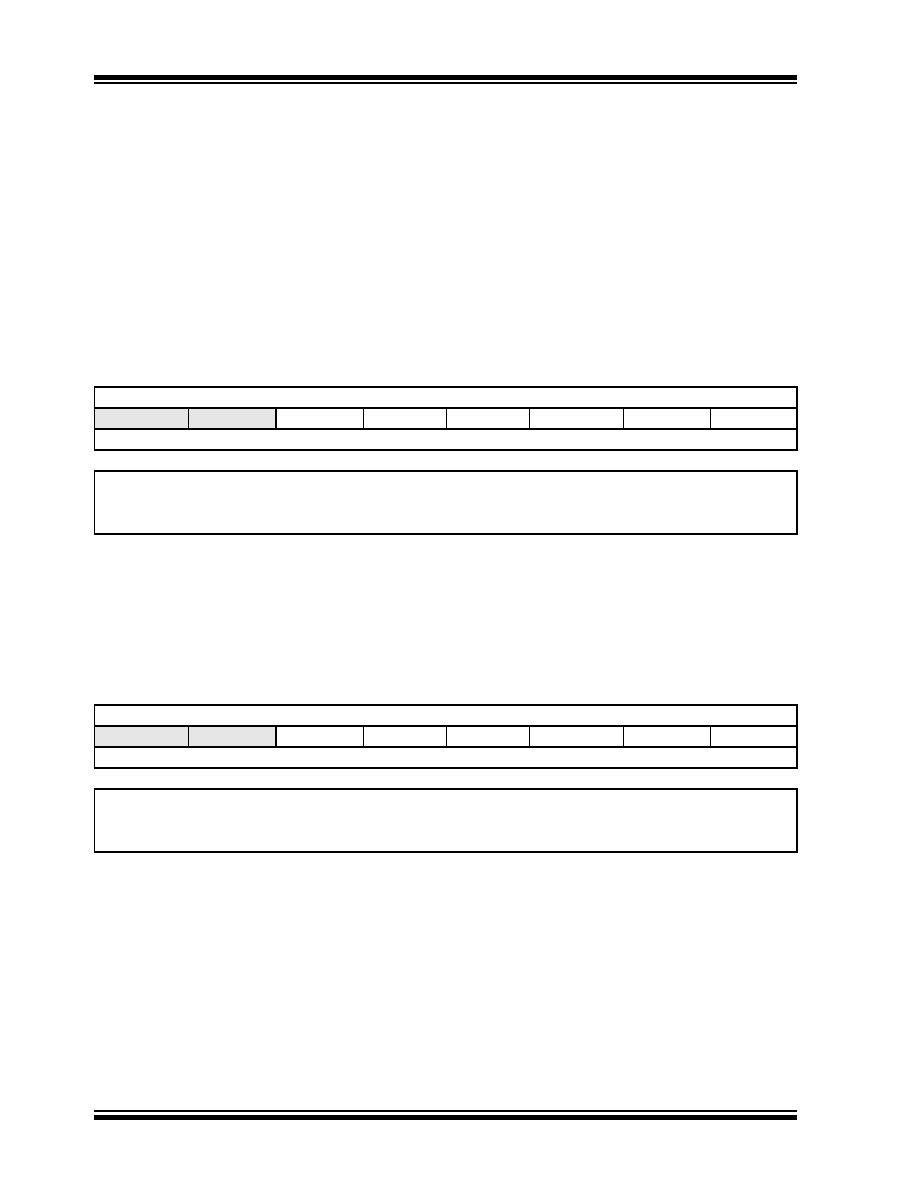
REGISTER 14-6:
OVDCOND: OUTPUT OVERRIDE CONTROL REGISTER
U-0
R/W-1
—
POVD5
POVD4
POVD3
POVD2
POVD1
POVD0
bit 7
bit 0
Legend:
R = Readable bit
W = Writable bit
U = Unimplemented bit, read as ‘0’
-n = Value at POR
‘1’ = Bit is set
‘0’ = Bit is cleared
x = Bit is unknown
bit 7-6
Unimplemented:
Read as ‘0’
bit 5-0
POVD5:POVD0:
PWM Output Override bits
1
= Output on PWM I/O pin is controlled by the value in the Duty Cycle register and the PWM time base
0
= Output on PWM I/O pin is controlled by the value in the corresponding POUTx bit
REGISTER 14-7:
OVDCONS: OUTPUT STATE REGISTER
U-0
R/W-0
—
POUT5
POUT4
POUT3
POUT2
POUT1
POUT0
bit 7
bit 0
Legend:
R = Readable bit
W = Writable bit
U = Unimplemented bit, read as ‘0’
-n = Value at POR
‘1’ = Bit is set
‘0’ = Bit is cleared
x = Bit is unknown
bit 7-6
Unimplemented:
Read as ‘0’
bit 5-0
POUT5:POUT0:
PWM Manual Output bits(1)
1
= Output on PWM I/O pin is active when the corresponding PWM output override bit is cleared
0
= Output on PWM I/O pin is inactive when the corresponding PWM output override bit is cleared
Note 1:
With PWMs configured in complementary mode, even PWM (PWM0, 2, 4) outputs will be
complementary of the odd PWM (PWM1, 3, 5) outputs, irrespective of the POUT bit
setting.
发布紧急采购,3分钟左右您将得到回复。
相关PDF资料
PIC18F1330T-I/ML
IC PIC MCU FLASH 4KX16 28QFN
PIC18F65J50T-I/PT
IC PIC MCU FLASH 16KX16 64TQFP
PIC18F83J11T-I/PT
IC PIC MCU FLASH 4KX16 80TQFP
PIC16LF627-04/P
IC MCU FLASH 1KX14 COMP 18DIP
PIC18F86J55T-I/PT
IC PIC MCU FLASH 48KX16 80TQFP
PIC18F43K22-I/MV
MCU PIC 8KB FLASH 40QFN
PIC16C55A-04I/P
IC MCU OTP 512X12 28DIP
PIC18LF43K22-I/MV
MCU PIC 8KB FLASH 40UQFN
相关代理商/技术参数
PIC18F1230T-I/SS
功能描述:8位微控制器 -MCU 4KB Flash 256 RAM RoHS:否 制造商:Silicon Labs 核心:8051 处理器系列:C8051F39x 数据总线宽度:8 bit 最大时钟频率:50 MHz 程序存储器大小:16 KB 数据 RAM 大小:1 KB 片上 ADC:Yes 工作电源电压:1.8 V to 3.6 V 工作温度范围:- 40 C to + 105 C 封装 / 箱体:QFN-20 安装风格:SMD/SMT
PIC18F1320-E/ML
功能描述:8位微控制器 -MCU 8KB 256 RAM 16 I/O RoHS:否 制造商:Silicon Labs 核心:8051 处理器系列:C8051F39x 数据总线宽度:8 bit 最大时钟频率:50 MHz 程序存储器大小:16 KB 数据 RAM 大小:1 KB 片上 ADC:Yes 工作电源电压:1.8 V to 3.6 V 工作温度范围:- 40 C to + 105 C 封装 / 箱体:QFN-20 安装风格:SMD/SMT
PIC18F1320-E/P
功能描述:8位微控制器 -MCU 8KB 256 RAM 16 I/O RoHS:否 制造商:Silicon Labs 核心:8051 处理器系列:C8051F39x 数据总线宽度:8 bit 最大时钟频率:50 MHz 程序存储器大小:16 KB 数据 RAM 大小:1 KB 片上 ADC:Yes 工作电源电压:1.8 V to 3.6 V 工作温度范围:- 40 C to + 105 C 封装 / 箱体:QFN-20 安装风格:SMD/SMT
PIC18F1320-E/SO
功能描述:8位微控制器 -MCU 8KB 256 RAM 16 I/O RoHS:否 制造商:Silicon Labs 核心:8051 处理器系列:C8051F39x 数据总线宽度:8 bit 最大时钟频率:50 MHz 程序存储器大小:16 KB 数据 RAM 大小:1 KB 片上 ADC:Yes 工作电源电压:1.8 V to 3.6 V 工作温度范围:- 40 C to + 105 C 封装 / 箱体:QFN-20 安装风格:SMD/SMT
PIC18F1320-E/SS
功能描述:8位微控制器 -MCU 8KB 256 RAM 16 I/O RoHS:否 制造商:Silicon Labs 核心:8051 处理器系列:C8051F39x 数据总线宽度:8 bit 最大时钟频率:50 MHz 程序存储器大小:16 KB 数据 RAM 大小:1 KB 片上 ADC:Yes 工作电源电压:1.8 V to 3.6 V 工作温度范围:- 40 C to + 105 C 封装 / 箱体:QFN-20 安装风格:SMD/SMT
PIC18F1320-H/ML
功能描述:8位微控制器 -MCU 8KB FL 256RAM 16 I/O RoHS:否 制造商:Silicon Labs 核心:8051 处理器系列:C8051F39x 数据总线宽度:8 bit 最大时钟频率:50 MHz 程序存储器大小:16 KB 数据 RAM 大小:1 KB 片上 ADC:Yes 工作电源电压:1.8 V to 3.6 V 工作温度范围:- 40 C to + 105 C 封装 / 箱体:QFN-20 安装风格:SMD/SMT
PIC18F1320-H/P
功能描述:8位微控制器 -MCU 8KB FL 256RAM 16 I/O RoHS:否 制造商:Silicon Labs 核心:8051 处理器系列:C8051F39x 数据总线宽度:8 bit 最大时钟频率:50 MHz 程序存储器大小:16 KB 数据 RAM 大小:1 KB 片上 ADC:Yes 工作电源电压:1.8 V to 3.6 V 工作温度范围:- 40 C to + 105 C 封装 / 箱体:QFN-20 安装风格:SMD/SMT
PIC18F1320-H/SO
功能描述:8位微控制器 -MCU 8KB FL 256RAM 16 I/O RoHS:否 制造商:Silicon Labs 核心:8051 处理器系列:C8051F39x 数据总线宽度:8 bit 最大时钟频率:50 MHz 程序存储器大小:16 KB 数据 RAM 大小:1 KB 片上 ADC:Yes 工作电源电压:1.8 V to 3.6 V 工作温度范围:- 40 C to + 105 C 封装 / 箱体:QFN-20 安装风格:SMD/SMT